Catching the Waves: Researchers blend novel materials to capture more energy from the sun
Researchers blend novel materials to capture more energy from the sun
The nanoscale crystals and quantum dots Ganesh Balakrishnan creates are mere nanometers in diameter, but they could help next generation solar cells harness more power from the sun by collecting light of different colors or wavelengths.
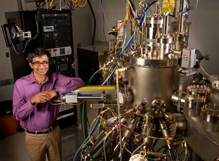
Photo: Ganesh Balakrishnan uses the molecular beam epitaxy machine to create novel wafers that could be used as solar cells.
Balakrishnan, assistant professor of electrical and computer engineering, leads a materials research group at the Center for High Technology Materials (CHTM). The team is combining dissimilar materials to create high efficiency, low cost solar cells. “We’re trying something fundamentally new as we work on next generation solar cell technology,” says Balakrishnan.
Their goal is to integrate semiconductors that absorb different wavelengths of light into a single material by developing new techniques to manipulate crystal growth. Standard solar cell technology made from silicon uses a single crystal that catches only part of the spectrum.
“Solar energy is very broad spectrum light, which means it has lots of different wavelengths or colors,” explains Balakrishnan. “If you can stack different materials on top of each other, the first layer could capture the first part of the spectrum and the second layer could capture the second.” The wafers of novel materials Balakrishnan develops could be used as solar cells in compact but powerful solar arrays on rooftops or other small spaces.
In one research project, Balakrishnan is collaborating with scientists from the National Renewable Energy Laboratory to grow crystals of gallium antimonide, a family of relatively expensive compounds, on a substrate of inexpensive gallium arsenide or silicon.
The substrate absorbs the visible and ultraviolet part of the spectrum while the gallium antimonide absorbs the invisible infrared spectrum.
He’s applying the same idea but using different structures in a second project where he’s anchoring quantum dots of a gallium antimonide on a substrate, then surrounding the dots with gallium arsenide.
Decades of Expertise
Balakrishnan uses CHTM’s molecular beam epitaxy (MBE) machines to create these novel materials. The MBE allows researchers to build precise layers of semiconductors by growing one atomic layer at a time.
“CHTM has one of the best MBE labs in the world for quantum dots and antimonide semiconductors,” says Balakrishnan. “Such dominance in these two research fields can be traced to several decades of cutting-edge epitaxial research by faculty members such as Steve Brueck, Ralph Dawson, Luke Lester, Sanjay Krishna, and Kevin Malloy.”
Balakrishnan’s novel materials find their way into a collaborative network of faculty members working in the area of photovoltaics. The team led by Luke Lester, interim chair and professor of electrical and computer engineering, fabricates the semiconductors into working solar cells and also tests them in his solar cell laboratory. Olga Lavrova, assistant professor of electrical and computer engineering, works very closely with the two teams to implement the solar cells into systems.
In the future, these low cost, high efficiency solar cells could be on rooftops near you, pulling more power out of every ray of the sun and helping fuel a clean energy future.